
Capabilities
Deposition, processing, and analysis — under one roof.
Use the tools yourself as a trained facility user, or engage our team for process development, prototyping, and production services.
User Facility — Deposition & Processing
Hands-on, open-access instrumentationSputter Deposition
Multiple magnetron sputter systems for thin-film research and development
Thermal Evaporation
Vacuum thermal evaporators for metals and organic thin films
Heat Treatment
High-temperature vacuum ovens for annealing and materials processing
Vacuum Thin-Film Processes
Specialized vacuum processing for advanced film architectures
Plasma Treatment
Surface activation, cleaning, and modification
Batch Production
In-line multi-target sputter system for substrates up to 48" wide — feasibility to pilot scale
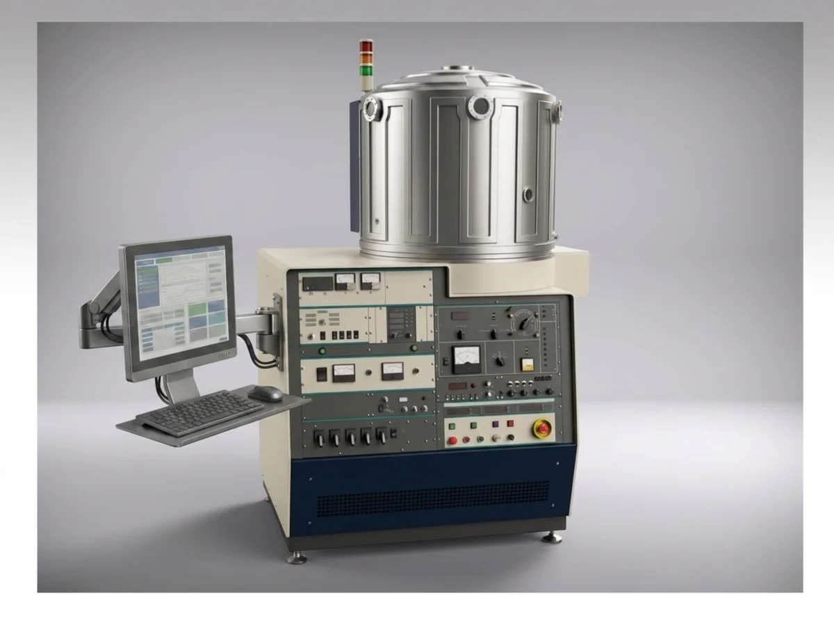
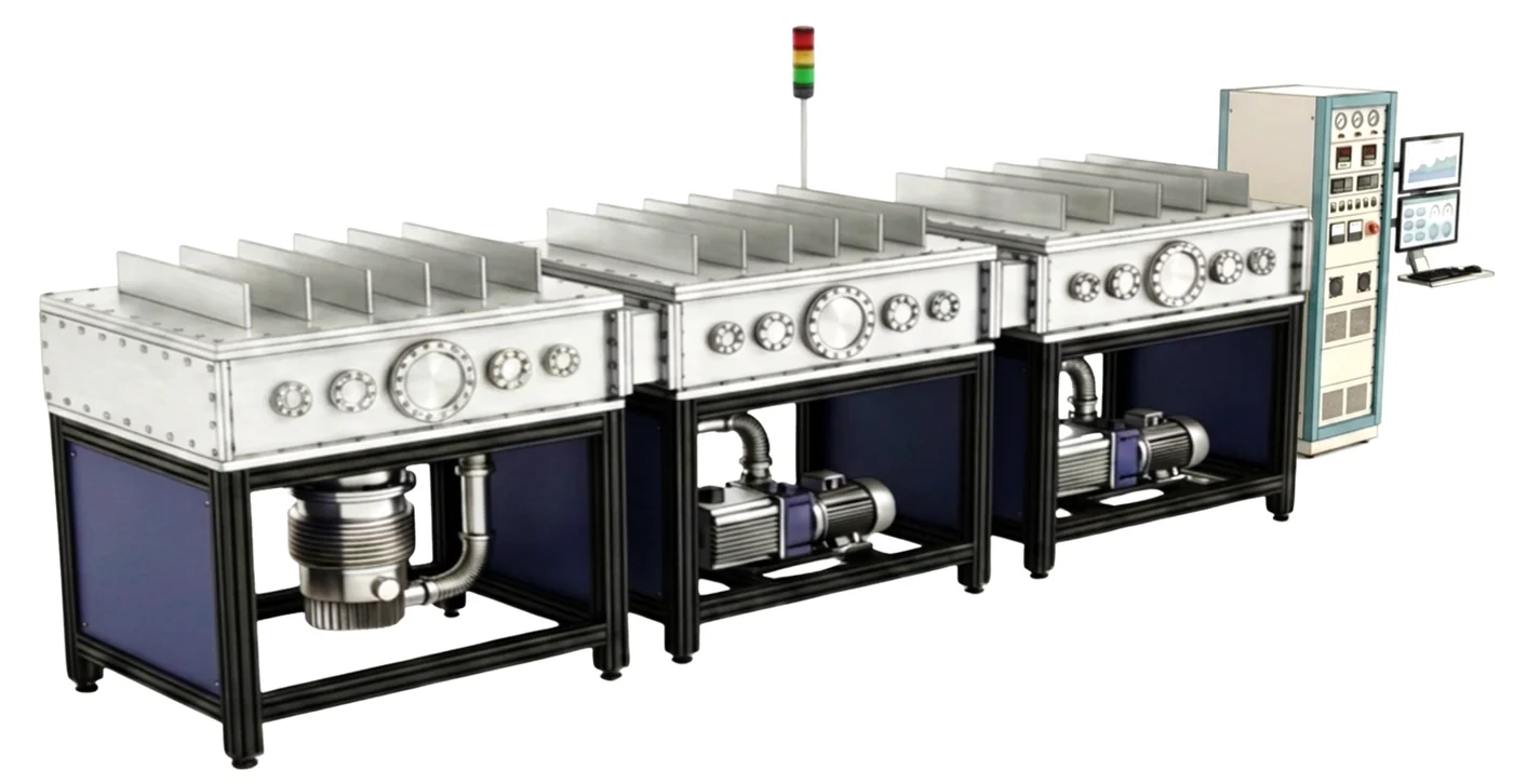
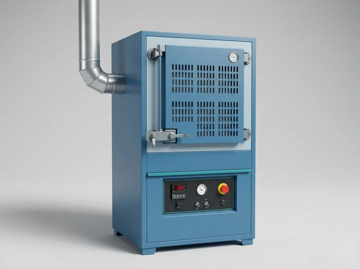
Equipment illustrations depict systems as commissioned; installation and commissioning are underway at our Loveland facility.
Analytical & Characterization Services
Full-service analysis by expert staff
SEM Imaging
Surface morphology, grain structure, and film coverage at high magnification. Useful for checking film quality, grain size, pinholes, and coating uniformity.
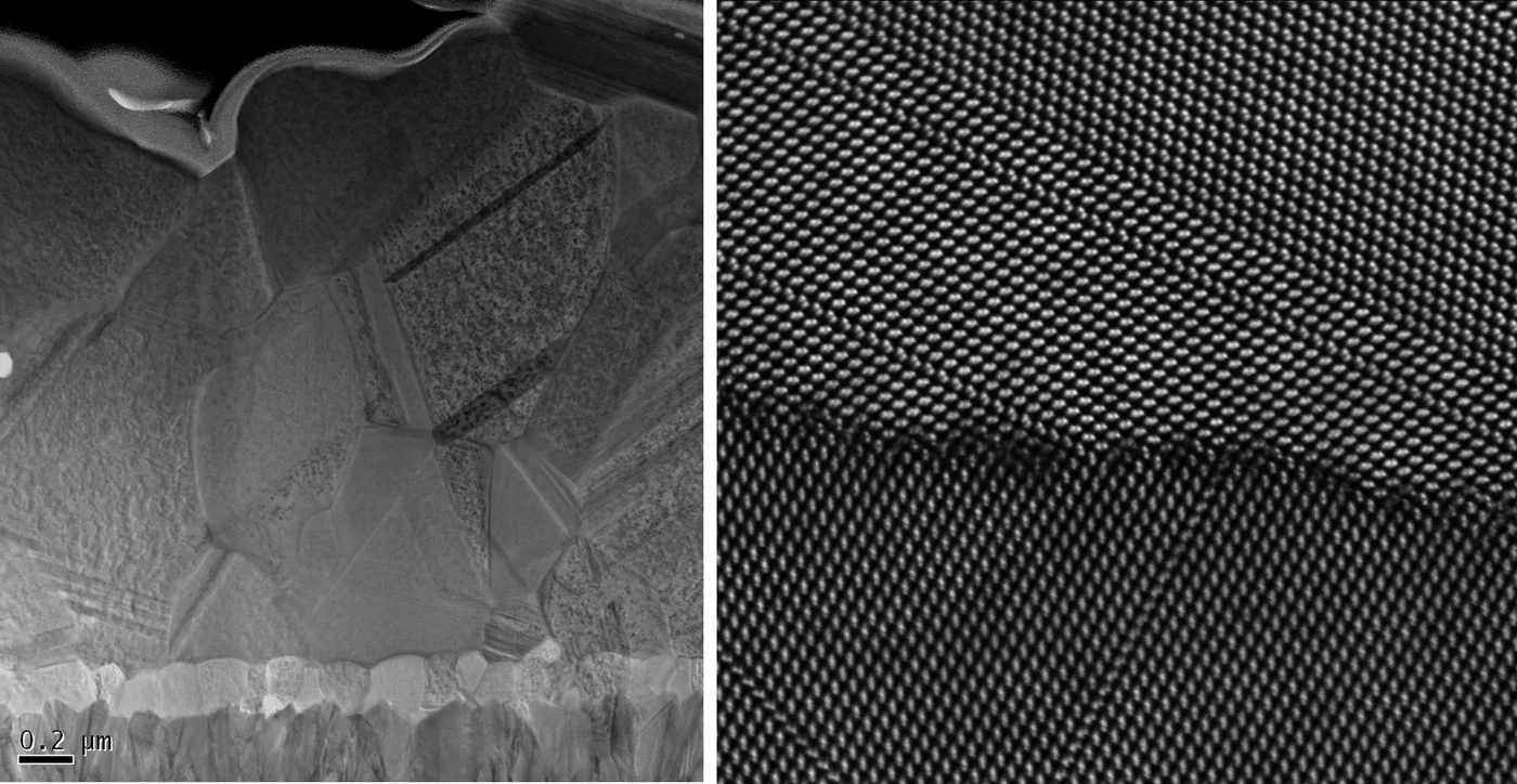
TEM Imaging
Cross-sectional imaging from nanometer scale down to individual atomic planes. Useful for layer thickness, interfaces, defects, and atomic-scale film structure.
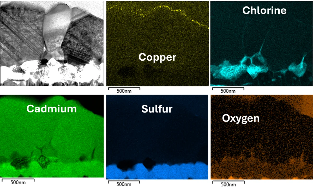
EDS Mapping
Nanoscale elemental mapping and composition analysis across layers and interfaces. Useful for verifying layer chemistry, interdiffusion, and dopant or impurity distribution in film stacks.
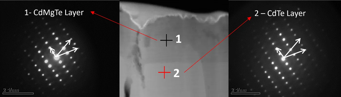
Electron Diffraction
Crystal-structure analysis from selected nanoscale regions of a specimen. Useful for phase identification, crystallinity, and orientation of thin films, interfaces, and individual grains.
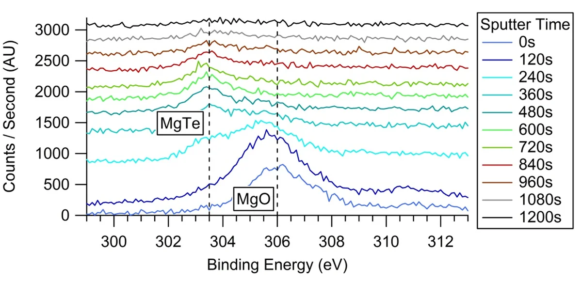
X-ray Photoelectron Spectroscopy
Surface-sensitive chemical analysis and depth profiling through film stacks. Useful for layer composition, chemical bonding states, interface sharpness, and surface contamination.
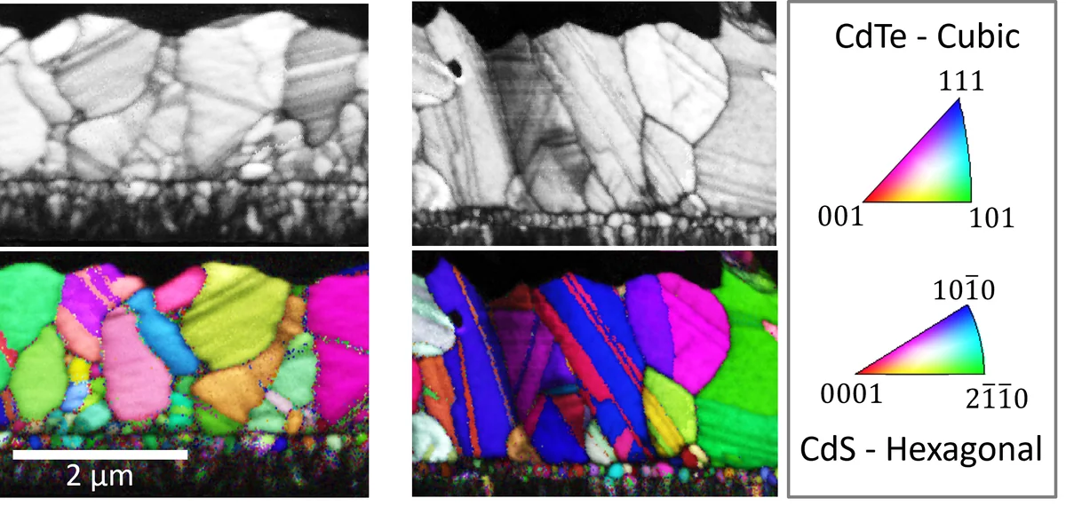
EBSD
Color-coded crystal-orientation maps of polycrystalline films. Useful for grain size, texture, and grain-boundary analysis that drives film performance.
Other Capabilities
- ICP-MS
- FTIR
- FTIR Microscopy
- XRD — Powder XRD · Single Crystal XRD · Multipurpose XRD
- SEM — SEM Analysis · EDS · EBSD · CL
Expert Services
Process Development
Custom thin-film process design, optimization, and scale-up support. Useful for turning a materials idea into a repeatable, documented recipe — deposition parameters, thermal treatments, and metrology.
Prototyping & Feasibility
Batch production of thin films for testing, validation, and proof-of-concept. Useful for de-risking a product idea — sample quantities for customer evaluation and manufacturing-feasibility data before you invest in equipment.
Consultation
Expert guidance on materials selection, deposition strategy, and characterization planning. Useful when you need decades of thin-film experience before committing to a process, tool, or analysis path.
Have a process to develop or a film to make?
Tell us what you're building. We'll tell you how STARC can help.
Start the ConversationDeposition & Processing Equipment
The full complement of thin-film deposition and thermal-processing tools available to trained facility users and through staff-performed services.
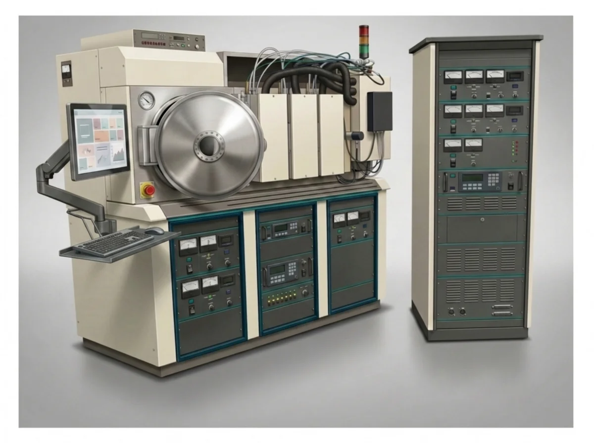
MRC Sputter Systems
Two three-target MRC sputter systems for research-scale DC and RF magnetron deposition of metals and compounds. The workhorses for recipe development, multilayer stacks, and small-batch coating runs.
Mag-Drum Sputter System
Three planar magnetron sources (one RF, two DC) with drum-mounted substrates and radiative substrate heating. Handles flexible substrates and glass — ideal for uniform contact layers, barrier films, and coating development over large areas.
In-line Batch Sputter Line
A 20-ft in-line system with up to twelve targets, in-situ substrate heating, and chain-driven transport for substrates up to 48″ wide. Bridges the gap between lab samples and production — pilot runs, batch device stacks, and manufacturing-feasibility studies.
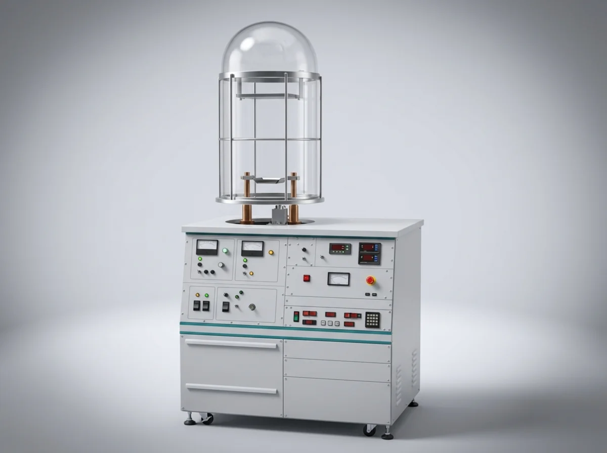
Thermal Evaporators
Vacuum thermal evaporators including a bell-jar system with a 12″×12″ uniform deposition area. Resistive-boat evaporation for metallization — back contacts, electrodes, and metal interlayers.
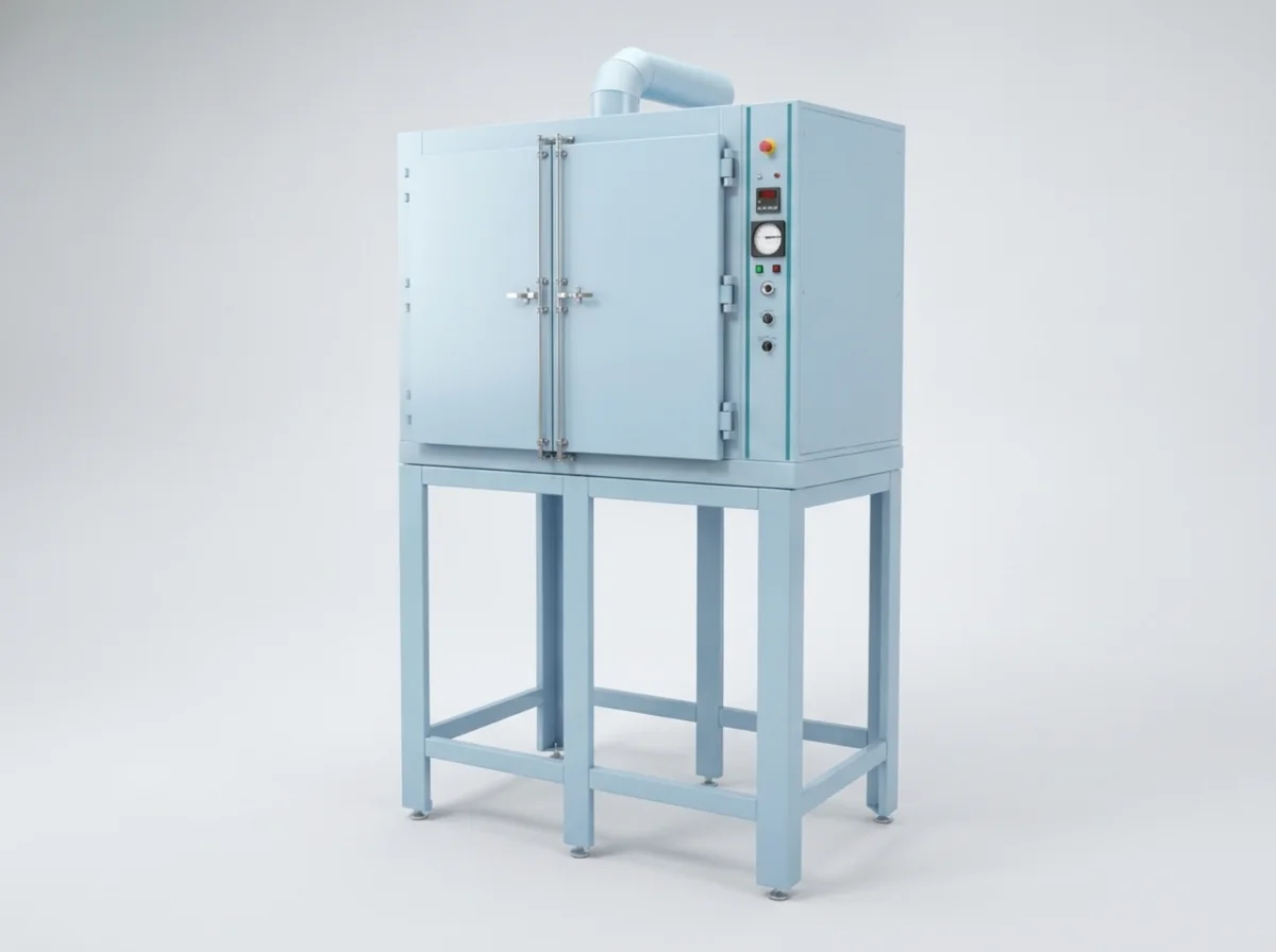
Large High-Temperature Furnace
A 24-ft³ double-door convection furnace reaching 593 °C. Sized for batch post-deposition treatments — annealing, film crystallization, and thermal processing of large substrate loads.
Compact High-Temperature Furnace
A 5-ft³ convection furnace to 538 °C for smaller batches — annealing studies, dopant activation, and process-development heat treatments where fast turnaround matters.
Equipment illustrations depict systems as commissioned; installation and commissioning are underway at our Loveland facility.
Advanced Electron Microscopy & Nanoscale Analysis
Beyond imaging, our electron-microscopy services resolve chemistry, crystallography, and atomic-scale defects in thin films — the details that determine how a material actually performs.
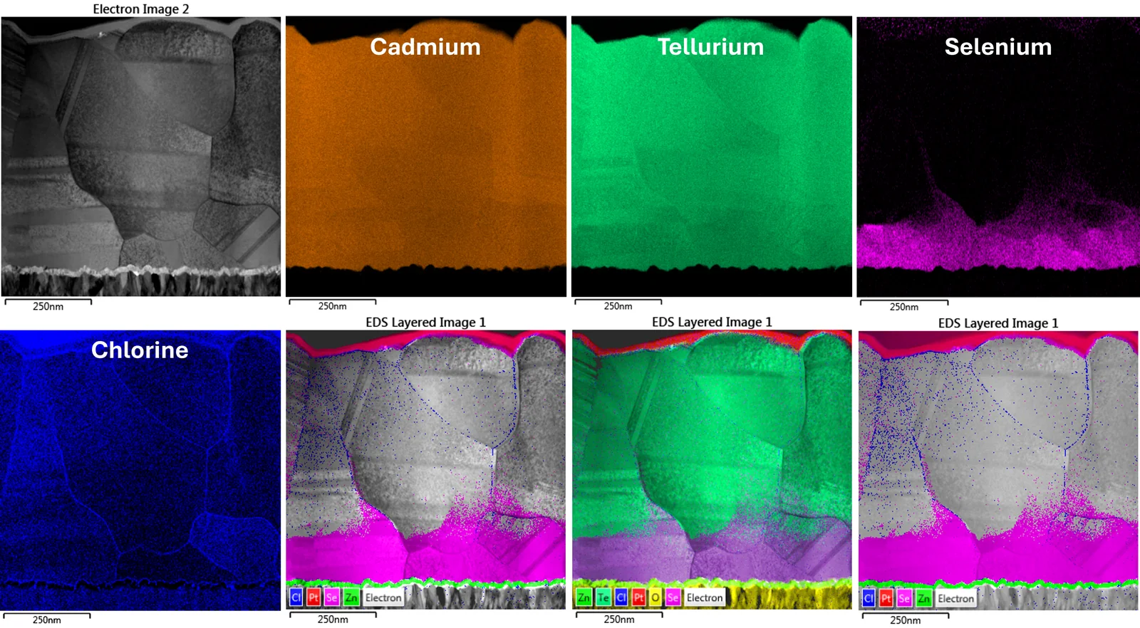
TEM-EDS Elemental Mapping
Color-coded maps showing where each element sits in a specimen at nanometer resolution. Reveals layer chemistry, interdiffusion, segregation to grain boundaries, and unexpected impurities.
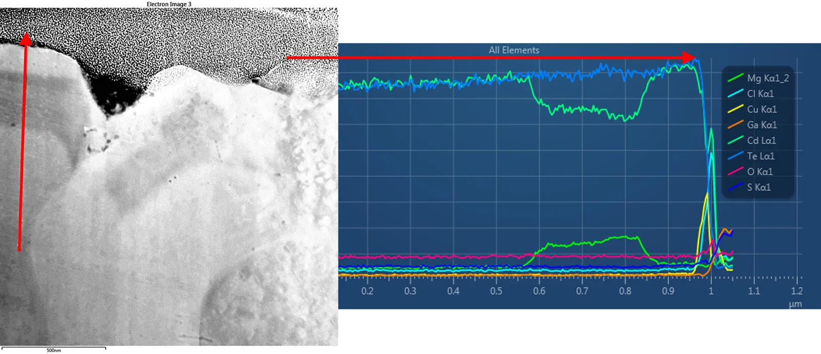
TEM-EDS Line Scans
Quantitative composition profiles along a line across layers and interfaces — a direct measurement of layer thickness, interface sharpness, and elemental gradients.
EBSD Orientation Mapping
Electron backscatter diffraction maps every grain's crystal orientation across a film. Quantifies grain size, texture, and grain-boundary character — key drivers of electrical and mechanical performance.
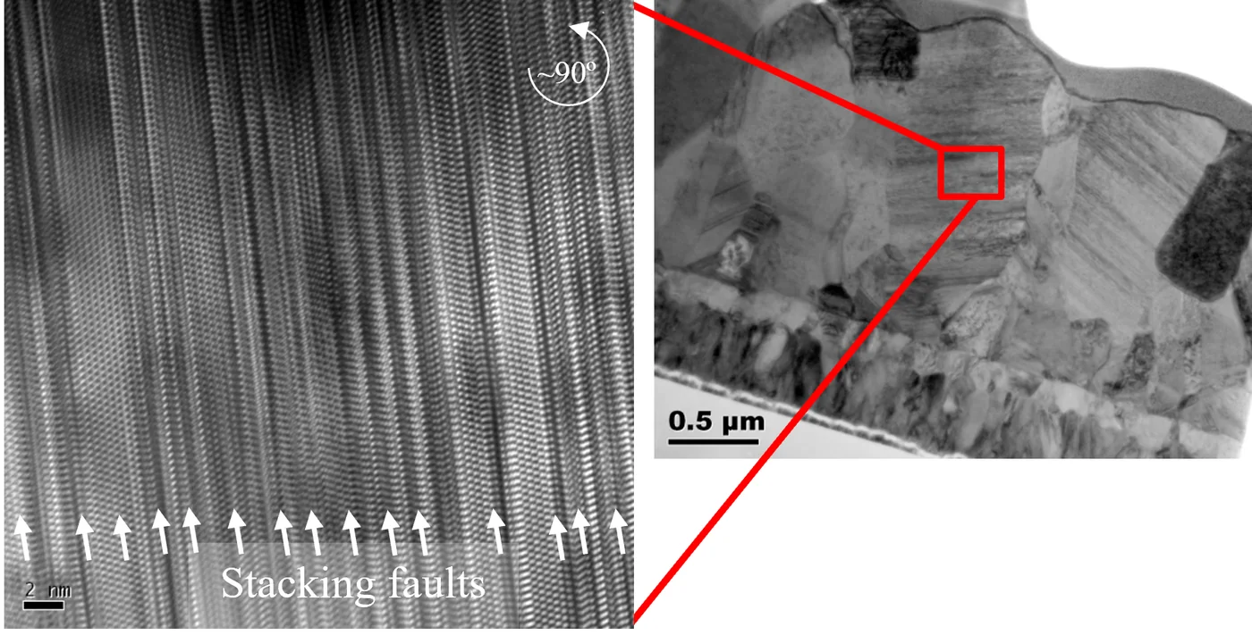
HRTEM — Stacking Faults
Atomic-resolution imaging of planar defects where the crystal's stacking sequence is interrupted. Identifying and counting these defects explains carrier losses and guides process fixes.
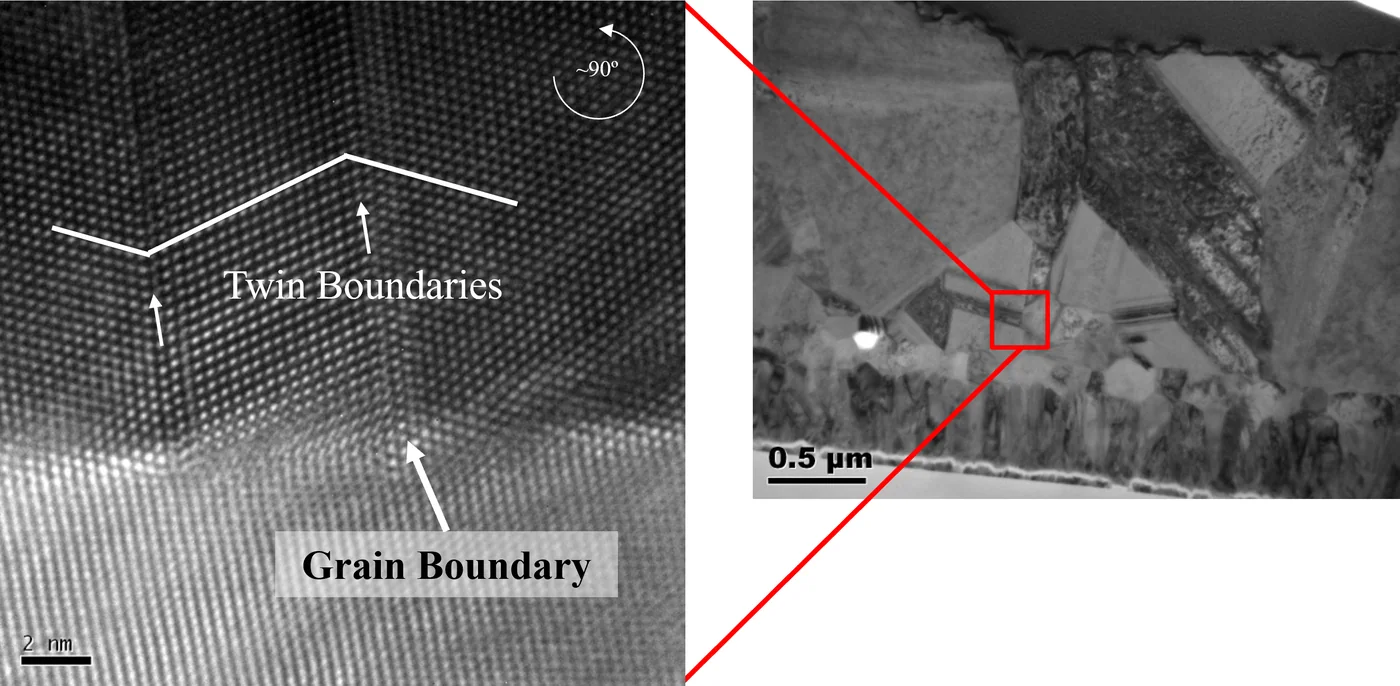
HRTEM — Twin Boundaries
Atomic-scale imaging of twin boundaries — mirror-image crystal domains within a grain. Understanding twinning distinguishes benign boundaries from performance-limiting defects.
FIB Specimen Preparation
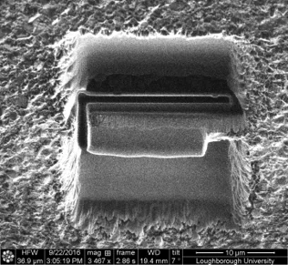
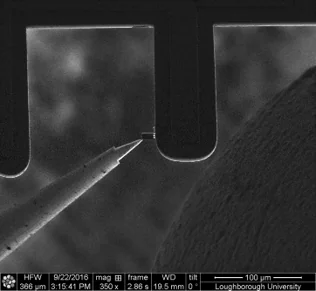
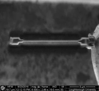
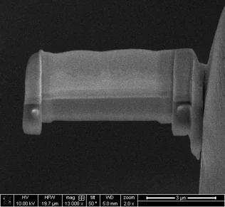
A focused ion beam (FIB) mills an ultra-thin cross-section — a lamella — from the exact spot you care about: a specific grain boundary, interface, or device feature. The lamella is lifted out, mounted on a grid, and thinned until electrons can pass through it, making site-specific TEM analysis possible. It's how a question like "what does this interface look like?" gets answered at the atomic scale.